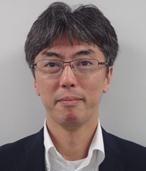


Biography: Osamu Nakatsuka was born in Osaka, Japan, in 1972. He received the BS degree in applied physics, the MS and Ph.D degrees in crystalline materials science from Nagoya University, Japan, in 1995, 1997, and 2000, respectively.
In 2000, he joined the Venture Business laboratory, Kyoto University, Japan as Postdoctoral Fellow and was engaged in the development of metal/SiC contact technology. In 2001, he moved to the Center for Integrated Research in Science and Engineering, Nagoya University, Japan, and was engaged in the research and development of materials and process technology for Si MOSFET applications. From 2006 to 2011, he was a Visiting Research Fellow in Japan Synchrotron Radiation Research Institute, Japan. From 2010, he was an Associate Professor in the Department of Crystalline Materials Science, Graduate School of Engineering, Nagoya University. From 2015 to 2016, he was a Visiting Associate Professor in the Department of Electrical Engineering, Stanford University, USA.
From 2016, he is a Professor in Graduate School of Engineering, Nagoya University, and currently engages in the research and development of thin film growth and interface engineering related to group-IV semiconductors for Si nanoelectronics. He is a member of the Japan Society of Applied Physics, the Surface Science Society in Japan, and the Vacuum Society of Japan.
Speech Title: Development of GeSn and related semiconductor thin films for next generation optoelectronic applications
Abstract: GeSn and related group-IV semiconductor materials have much attractive for applications of next generation silicon nanoelectronics. GeSn has a unique properties promising energy band engineering for electronic and optoelectronic devices because it realizes the indirect-direct crossover with increasing a Sn content as high as 10% and/or inducing the crystalline strain. However, there are many challenges for realizing practical electronics applications, those are developments of the crystal growth, defect/doping control, energy band engineering, and controlling the interface properties. In our presentation, we will present our recent achievements of the crystal growth technology of GeSn, SiGeSn, and related semiconductor thin films. Also, we will introduce our recent development of the low resistance metal/Ge contact using GeSn-related interlayers for controlling the Schottky barrier height.
Keywords: Germanium, Tin, Epitaxial growth, Interface, Integrated circuits